
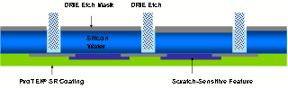
The demand for microelectromechanical systems (MEMS) requiring tall structure designs, as well as the increased density and performance expectations from the IC industry, are driving the need to utilize deep reactive ion etching (DRIE) in creating deep anisotropic etches of silicon for MEMS and semiconductor device applications. Vast yield hits are frequently the outcome of this process, where it is necessary to subject the front side of the substrate containing fragile, etch-sensitive circuitry to direct contact against the interior chuck of the etch chamber.
DRIE Advantages
Backside DRIE processes offer significant advantages over silicon wet-etch processes because of their ability to create very deep anisotropic vias. This ability allows manufacturers to maintain their target feature sizes during the entire etch. The DRIE process is frequently performed on substrates that have been previously subjected to costly processing steps necessary to create intricate device circuitry. These sensitive device features can be easily damaged as a result of undergoing the intense bombardment of plasma to the backside of the substrate. Additional benefits of DRIE processes include an increase in computational capacity utilizing flexible interconnects, increased electrical performance through shorter wire runs, and lower costs than existing CMOS techniques.
DRIE Applications
The backside DRIE process is used in MEMS to create devices such as microfluidics (ink-jet heads, BioMEMS), silicon microphones, pressure sensors, inertial sensors (gyroscopes, accelerometers), and other sensing and actuation devices. Increasingly, the DRIE process is used in CMOS to create through-wafer interconnects for packaging, chip stacking, and system-in-package (SiP) devices.
DRIE Solutions
Providing maximum protection for fragile, etch-sensitive circuitry placed in direct contact with the interior chuck of the etch chamber is critical. Photoresists have been used but they do not provide scratch resistance and are difficult to remove. Using a spin-applied polymeric coating that offers durability and longevity against the harsh, grueling backside DRIE processes is a viable solution.
Enabling DRIE Processes
A multitude of applications and industrial processes utilize backside DRIE processes. No longer is this type of etching process limited to MEMS devices such as gyroscopes, accelerometers, inertial sensors, or other membrane applications in sensing and actuation. DRIE processes are enabling the creation of CMOS processes where the MEMS devices can co-exist with integrated circuitry.


Subscribe to Our Blog