
Fabrication of microelectronic devices increasingly involves the creation of high-aspect-ratio structures (those with large height or depth and narrow width, such as trenches, vias, columns, and mesas). These structures provide isolation; serve as conduits for electrical, optical, or fluid signals; or enable pre-dicing before die singulation. New designs in semiconductor and MEMS devices are pushing the aspect ratios to the 10:1 range. For semiconductors, these designs may take the form of trenches 600 nm deep and 60 nm wide. For MEMS, these may be vias 500 µm deep and 50 µm in diameter. After these structures are created, additional photolithographic processing of the wafers is necessary. The technology to create these high-aspect-ratio structures, however, has outpaced the ability of existing technologies to process photoresists over them. This disparity has created a demand for materials that can level the surface of these processed wafers so that subsequent conventional photolithography processes can be used.
Many methods exist to planarize substrates, but three are compatible with a standard lithography track: the dry-etch-back, wet-develop-back, and expose-and-develop methods.
Dry-etch-back method
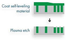 The dry-etch-back method of planarizing is straightforward. Typically an organic film is coated on the wafer. This material must have self-leveling properties to minimize the difference in overburden between areas with high feature density and areas with low feature density.
Overburden is the thickness of material extending beyond the top of the trenches. Self-leveling is the tendency of the material to flow or re-flow during processing to create a uniform, flat surface across the wafer.
Once the material is coated and baked, the wafer is placed in a dry-etch chamber and oxygen ashed to remove the overburden.
The advantage to this method is that a wide range of materials can be used. Depending on the selection of the material, the methods for removing the fill include dry etching, wet etching (with solvent or developer), or thermal decomposition.
The disadvantage of this method is that it does require a dry-etching tool. Also, during the dry-etch-back process, other organic films on the substrate may be damaged.
Wet-develop method
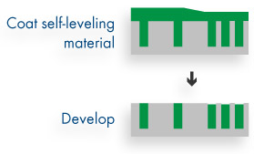 The next method of planarizing a substrate is wet developing. This method is similar to the dry-etch-back process except that TMAH developer or a solvent is used to remove the overburden. For many of our materials, we find that the etch rate of the overburden material is much faster than the etch rate of the material in the vias or trenches. This difference reduces the iso-dense variance.
An advantage of this method is that all the processing can be performed on a standard litho track. Also, the film can be later removed by the same wet processing. The disadvantage is that the ability to be removed in developer or solvent may limit downstream processing. In some cases, the material can be cured after developing so that it is no longer soluble. This, however, then limits later removal to dry etching only.
Expose-and-develop method
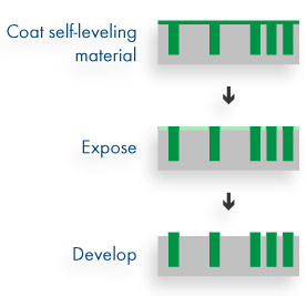 In the expose-and-develop method, a photosensitive material with self-leveling properties is used. The material is coated on the wafer and then baked. The wafer is then exposed by photolithography (the material is typically negative acting) to set the material in the vias or trenches. The overburden in the open areas is removed by either a TMAH developer or a solvent developer, depending on the planarizing material being used. After exposure, the material in the vias is normally removed by plasma etching.
Brewer Science offers many materials that can be used to level the surface of the substrate. Selecting the correct material depends on the scale of the structures (nanometer, micrometer, or millimeter), the aspect ratios, and the desired processing method.


Subscribe to Our Blog