
Defect reduction in advanced lithography can be achieved with Metrology. Metrology is the science of measuring, characterizing, and analyzing materials. Within metrology, there are several technologies used to detect material defects on a very small scale – precision on the scale of parts per trillion or less is necessary in our pursuit of zero defects at Brewer Science. Our approach to characterizing materials has been rigorously refined to give us the ability to measure and define our materials in a way that continues to surpass the expectations of our customers. We broadly define our characterization approach into three main categories: on wafer, in bottle and in situ.
On Wafer
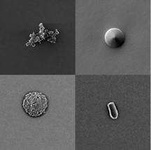
By making a large investment in a suite of cutting-edge surface analysis metrology tools, we can inspect our products just as our customers would. A standard methodology is post-coat defect analysis, which involves coating silicon wafers with our product and looking for any imperfections in the coating, down to as small as 20 nm. These are sized, counted, imaged and classified by type to create a defect baseline. We also stress the coating and curing processes in order to design out potential modes of failure. Additionally, we perform post-etch analysis, where we etch away the coatings with plasma to see if anything is left behind. Combined, these techniques allow us to design out the causes of defects by the manufacturing process, the product formulation, or even the product chemistry.
In Bottle
Characterizing the materials by impurity markers, in a process known as finger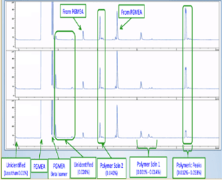 printing, allows us to classify the chemicals in our analytical lab. This allows us to detect impurities in raw materials, intermediate materials and final products.
In Situ
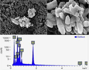
Particle detection in situ, or "in position,” involves looking at particles left behind on an experimental filter membrane in our high-resolution scanning electron microscope. This process involves identifying particles based on their morphology (size and shape) and also by discrete elemental analysis. These factors aid in finding the sources of particle defects and metal impurities, which we then eliminate under our Zero-Defect program.
Defect Reduction Roadmap
The process doesn’t stop here; at Brewer Science, we continually improve and seek innovative ways to detect and characterize defects. We are currently exploring new technologies to advance our capabilities and understanding in order to take materials to new measures, passing parts per trillion (PPT) and aiming for parts per quadrillion (PPQ).
Brewer Science is a global leader in developing and manufacturing advanced materials and monitoring systems for the reliable fabrication of cutting-edge micro-devices. We are passionate about sharing this knowledge on a fundamental level to help grow the understanding of semiconductors and metrology. Metrology and our characterization approach are tools we require to create a precise process, necessary to see defects on a parts per trillion scale and allow us to keep our promise of zero defects. Visit our website to learn more about the Zero Defect program.


Subscribe to Our Blog