
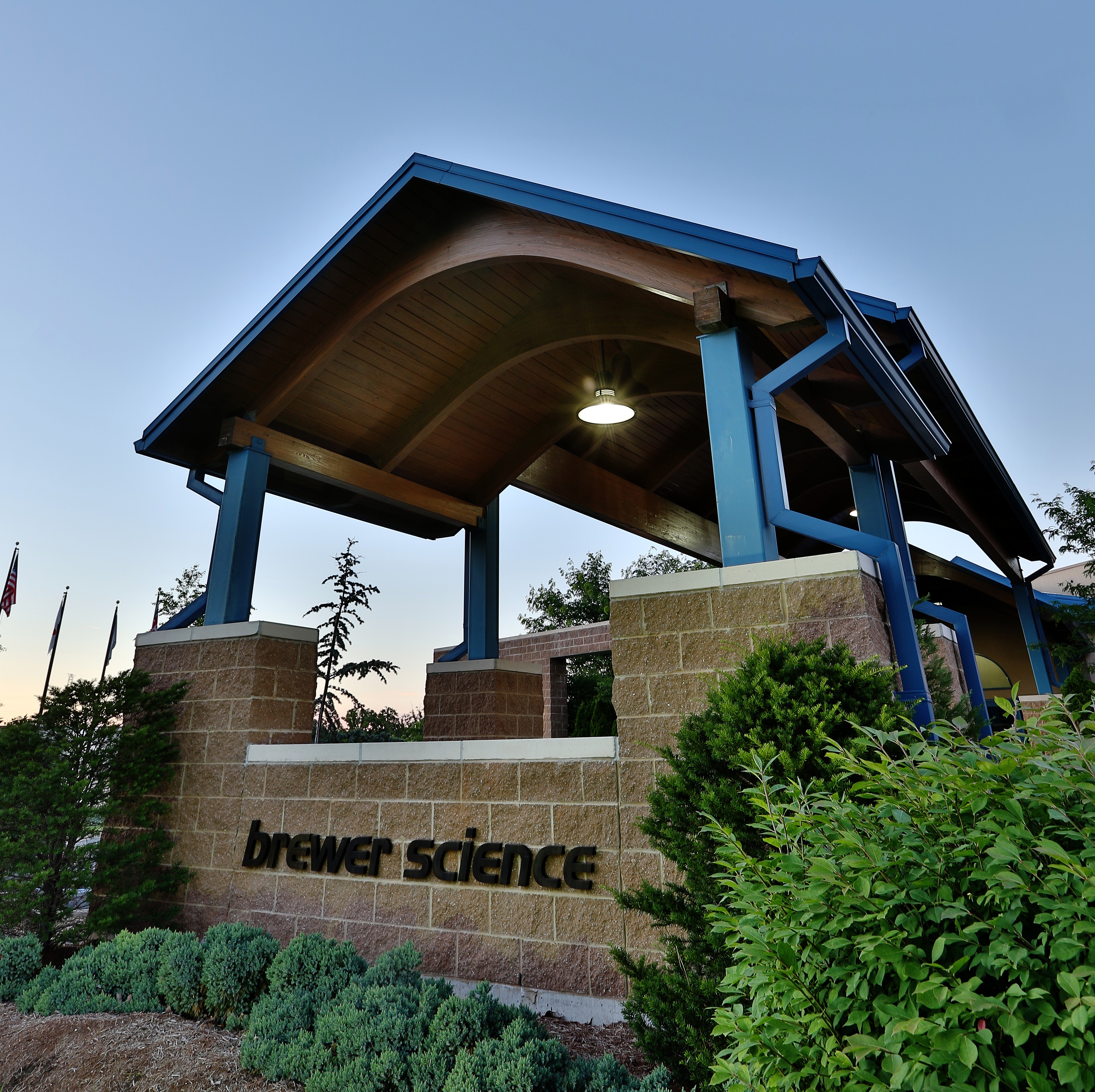
 Since our inception, Brewer Science has been strongly committed to cultivating diversity. And we do so for one primary reason: a broad range of backgrounds leads to better ideas and more innovation. But diversity in and of itself isn’t enough; we seek out truly unique talent that will bring the right mix of education, experience and raw intelligence to our company. We also believe this model starts at the top and that our senior management team should reflect the diversity we strive for across the organization.
With this in mind, we are proud to announce Rama Puligadda’s promotion to that team as executive director of Advanced Technologies R&D, to help run our rapidly growing Wafer-Level Packaging Materials business unit. In her new role, Rama will lead our Ph.D.-laden development team to drive products from concept to design to manufacturing.
Rama brings a strong background in chemistry, materials science, engineering expertise and leadership to her new role. She holds separate master’s degrees in chemistry, polymer science and technology, and chemical engineering. Rama joined Brewer Science in 1995 as a research chemist, and has rapidly risen through the ranks to lead several product development projects and collaborative partnerships with universities and research institutions.
It’s just those types of collaborations that Rama will be fostering with customers, as the need for innovation grows in the industry, and packaging technologies becoming an ever-more important driver. Semiconductor companies are increasingly looking to squeeze more intelligence into smaller and smaller packages, and this is where Rama and her team come in. Just as our groundbreaking anti-reflective coatings for lithography have enabled the front-end progression of Moore’s law since the 1980s, Brewer Science’s innovative wafer-level and panel-level materials are allowing chipmakers to break through advanced-packaging technological barriers on the back end.
One recent example of that innovation will be showcased in a paper that Rama will present in Raleigh, North Carolina, at the 50th Anniversary Symposium of the International Microelectronics Assembly and Packaging Society. Developed in collaboration with customer Suss MicroTec Group and titled “Ablative Laser Patterning of Polymeric Dielectric Materials,” her presentation will explain how new dielectric materials will enable crucial advancements in electronic packaging technology. Rama will present alongside Suss MicroTec and several members of her Brewer Science R&D team, at 8:30 a.m. on Wednesday, Oct. 11, 2017, in Raleigh Convention Center, Room 306C, as part of the symposium’s Advanced Materials and Processes track.
Rama and her colleagues will show that, as devices become smaller and lighter, new and improved dielectric materials are needed to continue packing more functionality into them. Current materials exhibit high cure temperatures and high stress, leading to delamination or warpage in the reconstituted wafers used for advanced packaging. Their paper will demonstrate how new dielectric materials with low cure temperatures, high elongation and low coefficients of thermal expansion can spur innovation in packaging that enables new applications.
If you’d like more information about the latest advances in semiconductor packaging, or to schedule a meeting with Rama at IMAPS, send us an email: info@brewerscience.com.

Subscribe to Our Blog