
Imagine you’ve decided to undertake a home improvement project; you’re going to lay tile in the downstairs powder room.
To begin, you remove the old vinyl flooring. Underneath are clumps and channels of dried adhesive atop a concrete slab foundation that looks like a miniature lunar landscape. In order to ensure your tiling project has the best chance of success, you need to smooth out the subfloor it will rest on. Failing to smooth the surface will result in an uneven floor and compromised tile that will crack and break over time.
Planarization in semiconductor manufacturing works in much the same way, except with much greater complexity of process and desired results. Plus, instead of a single surface to smooth, the topography of multiple layers comes into play. And it all happens on a scale so minuscule that even the tiniest variation in surface topography of any layer can vastly affect the success of the manufacturing process.
Of course, success and progress in the semiconductor industry have long been measured in how small we can make chips. However, the smaller you go, the less tolerance there is for variations in topography.
The importance of topography
Photolithography — the process of using light beams to create circuits on a silicon wafer layered with a photosensitive material — has made it possible to create smaller, highly complex, and multilayered microchips. However, roughness in any given layer can foul up the process by reflecting the light beams used in lithography, or preventing the light from achieving proper focus. When that happens, desired features won’t get printed on the chip.
As layers become thinner and the nodes where circuit elements meet become smaller, the surface smoothness of each layer becomes even more important. The process of turning those uneven surfaces into smooth, photolithography-friendly layers is called planarization.
The CMP solution
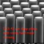
Historically, chemical-mechanical polishing (CMP), along with the use of filler materials, has been the most common process for planarizing in the semiconductor industry. However, CMP doesn’t work very well on organic films, and is used mainly for metal layers. What’s more, in the future, feature sizes for nodes will be even smaller, making it even more difficult to design a mask that considers the effect of substrate topography.
Brewer Science innovation
For more than 35 years, Brewer Science has been pioneering innovative solutions to the challenges of semiconductor manufacturing. We’ve developed a range of new planarizing spin-on materials with unique properties, including:
- OptiStack® PL700 material (and derivatives), a planarizing material designed to be "smart." On dark-field topography, baking the material causes the material to flow into the center of trenches, leading to zero, or even negative, bias. These materials can be tuned to have almost perfect planarization. Conventional spin-on carbon (SOC) materials have rather large positive bias over trenches.
- High-temperature (HT) planarizing SOCs are materials for advanced lithography applications. They are designed to have minimal bias after bake at 450°C such as during chemical vapor deposition (CVD) processes. They have minimal thermal shrink after CVD at extremely high temperatures — something very hard to achieve.
Brewer Science’s planarizing innovations solve the problem of high bias for future nodes. Current standard system-on-a-chip materials aren’t designed to be highly planarizing. They also don’t survive most CVD processes, and if they do, they are just gap-fill materials with no planarization.
These innovations in planarization can help ensure greater success for semiconductor manufacturing processes, ensuring every layer of a chip creates a smooth, even foundation for building smaller, complex, and powerful transistors.


Subscribe to Our Blog