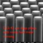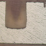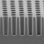


Over the past decade, Brewer Science has developed and published various methods of creating a planar surface over three-dimensional (3-D) structures. Sharing these results invariably leads to a potential customer asking, “Can you fill the holes in my substrate that are x in size?” The short answer to the question is “Yes, we can.” Filling holes, however, is rarely the only thing customers want to do. Typically they want to do something else, for instance, coat a photoresist, maintain chuck vacuum, support a structure, etc. That “something else” usually presents a challenge that is very different than just filling holes. For Brewer Science to provide the best solution for your particular structure and need, our highly experienced engineers and scientists must ask many more questions about what processes are acceptable and what downstream conditions the substrate must withstand.
To minimize cost and complexity, we offer process and material flexibility and compatibility with a standard photolithography track. We provide materials to level 3-D topography using the following methods:
Dry etch back
- Requires an etching tool and bay transfer
- Includes a variety of processes for which Brewer Science coatings are highly effective
Expose and develop
- Requires an exposure tool and a developer spin bowl
- Removes with dry etching
- Takes advantage of the very good chemical resistance offered by Brewer Science materials
Wet etch back
- Uses TMAH or solvent developer
- Requires a developer spin bowl
- Offers processing with no bay


Subscribe to Our Blog