
The device you are using right now—whether it be a phone, tablet or even a computer—is smaller than its predecessors, yet its capabilities are far greater than ever before. With the challenge to produce microchips on the smallest scale possible, manufacturers must devise a solution to protect fragile integrated circuits, while dissipating heat and increasing performance, all while connecting to the circuit board and other elements. This demanded the introduction of the innovative solution: wafer-level packaging.
What is Wafer-Level Packaging?
First let’s examine what wafer-level packaging (WLP) fundamentally is, and how it’s different from traditional forms of packaging. Wafer-level packaging is the technology of packaging the die while it is still on the wafer—protective layers and electrical connections are added to the substrate before dicing. Originally, wafers were diced into individual chips, then packaged.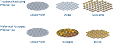
Imagine comparing WLP and traditional packaging to baked goods. Traditional packaging is like frosting individual cupcakes, whereas wafer-level packaging is like frosting an entire cake, and then slicing it into pieces. In WLP, the sides are not coated, thus is usually results in a smaller-sized packaged chip. This allows for smaller device applications. In addition to smaller devices, wafer-level packaging helps bring the cost down while allowing higher levels of integration.
Wafer-Level Chip-Scale Packaging (WLCSP)
WLP is known as chip-scale packaging (CSP) technology, as the resulting package is essentially the same size as the chip itself. In the industry, a chip is more commonly referred to as a die. A die is a small block of semiconducting material on which a functional circuit is fabricated. Integrated circuits are produced in large batches on a single wafer of electronics-grade silicon, and then diced into pieces, each die containing one copy of the circuit. Wafer-level chip-scale packaging (WLCSP) is the smallest package currently available on the market and is just a bare die with a redistribution layer (RDL) to rearrange the pins or contacts on the die so that they can be big enough and have sufficient spacing to be handled. The advantage of WLCSP is not only its cost-to-performance ratio, but also, its small die size—making it one of the most popular packaging techniques in the industry. However, with its small size comes the limiting factor of number of inputs and outputs (I/O).
Fan-Out and Fan-In Wafer-Level Packaging
The shortcomings of limited I/O in WLCSP are addressed with either fan-out wafer-level packaging (FOWLP) or fan-in wafer-level packaging (FIWLP), both of which allow for more external contacts while maintaining the small package and low power consumption. The key difference between FOWLP and FIWLP is the size of the interposer relating to the die. An interposer is basically an electrical connection, and its purpose is to spread a connection farther or reroute a connection to a different connection. Thus, an interposer on a die in FIWLP is usually the same size as the die itself, whereas in FOWLP the interposer is larger than the die. The video in this section, “What is Fan-Out Wafer-Level Packaging,” gives a more technical overview of this process.
The Future of Wafer-Level Packaging
As packaging demands are constantly evolving, the collaboration within the advanced packaging space is critical. It’s important to communicate throughout the supply chain and engage with customers to understand their products, and to be aware of their trends and advancements. Engagement in consortium activities help indicate and understand where the industry is going because innovation is not driven by one customer, industry or market segment. Consortia usually focus on the larger needs of the industry. Brewer Science engages with all parts of the supply chain in an effort to not only understand the future advancements of the semiconductor industry, but also because of our commitment to quality and maintaining our Zero Defects promise.
Wafer-level packaging technology allows chips to continue to reduce in size, streamlines manufacturing, and provides easier ways to test chip functionality. The limitations of WLP regarding the number of I/O are addressed in FOWLP and FIWLP, which continue to evolve and innovate. Since Brewer Science is a technology leader in innovation, part of the company’s strategy is to seek opportunities that create value in the long term by anticipating the future needs of technology and enabling customer to pave a road to continued growth.
Efficient ways of packaging now will enable advancements for years to come, including Brewer Science’s technology enabling the advancements of Ultrathin Wafers. Ultrathin wafers are superior to wafer-level packaging as they provide better heat dissipation and increased performance while decreasing power consumption and reducing form factor. You can learn more about ultrathin wafers and other advanced packaging solutions Brewer Science has to offer on the Brewer Science website or by contacting a Brewer Science expert to understand what solutions are best for your company.


Subscribe to Our Blog