
Article published in Chip Scale review's March - April 2018; Volume 22, Number 2 Issue
The semiconductor industry is in a new age where device scaling will not continue to provide the cost reductions or performance improvements at a similar rate to past years when Moore’s law was the guiding principle for IC scaling. The cost of scaling below 7 nm nodes is rising substantially and requires significant investment in capital equipment and R&D spending for next-generation lithography solutions. The demand for higher performance, smaller form factor, denser integration, and lower-cost devices is increasing more than ever due to significant progress made in products and services developed for consumer electronics, mobile devices, cloud computing, automotive, and various other applications. While the semiconductor industry continues to advance scaling of the integrated circuits, it is also turning to advanced packaging technologies to increase performance and integration while lowering costs.
One of the several challenges in heterogeneous integration is to bridge the gap in the I/Os available at the die level and the board level. At the die level, the trend has always been shrinking die sizes with increasing I/O density, so creative packaging technology is required to connect the dies to the board at such high I/O densities. Numerous evolving packaging technologies play a role in heterogeneous integration of devices, amongst which wafer-level fan-out (WLFO) packaging technology has been emerging as a dominant process. The WLFO process has been commercially deployed for several years with simple single-die designs, a single redistribution layer (RDL) on one side of a reconstituted wafer, and sparse silicon areas on thick reconstituted wafer profiles that resulted in thicker packages.
More recently, to address the performance, integration, and form-factor demands from the end-users, design and process complexity of fan-out packages has continued to increase with multi-die packages, integrated passives, multi-RDL layers, and also 3D fan-out packages while continuously reducing the package dimensions in the x, y, and z directions. As die-size, process complexity, and package complexity increase, yield becomes a critical element of the fan-out packaging process. The traditional fan-out process uses a chip-first/RDL-last approach where a reconstituted wafer is built using known good dies followed by RDL build up on top of the reconstituted wafer. As the complexity of the reconstituted wafer and RDL grows, this process is susceptible to yield loss at the RDL level where a known-good die (KGD) is located in a bad RDL location. The yield loss could be due to several factors, including die-shift, thermal expansion mismatch, poor lithography alignment, etc., resulting in the loss of an expensive KGD during the packaging process.
To avoid KGD loss during packaging, an alternate fan-out process was developed called RDL-first/chip-last fan-out packaging, where the RDL was first built on a carrier wafer and KGDs were placed on top of a known good RDL location thereby avoiding KGD loss. The RDL-first process also offers other advantages in terms of finer line/space dimensions for RDL to offer complex routing for denser device integration. In this paper, we present sacrificial laser release materials that support the development of RDL-first fan-out packaging by addressing some of the critical challenges encountered during the process.
FOWLP technology
As mentioned above, the fan-out wafer-level packaging (FOWLP) technology broadly has two major process categories; chip-first/RDL-last fan-out and RDL-first/chip-last fan-out. Advanced integration schemes in both of the process routes require some form of carrier-assisted process using a temporary bonding material.
Chip-first/RDL-last FOWLP
The chip-first fan-out process utilizes a wafer reconstruction process in which KGDs from the original device wafer are picked and placed on a substrate and then over-molded with an epoxy molding compound and cured to create a heterogeneous and highly stressed substrate known as a reconstituted wafer. If the reconstituted wafers are thinner than 350 µm, these wafers exhibit severe bow due to large internal stresses, and a high-temperature-capable temporary bonding material is essential to support the reconstituted wafer through the process flow [1] to reduce the bow and to alleviate handling problems in equipment and registration errors during alignment for photolithography during RDL build.
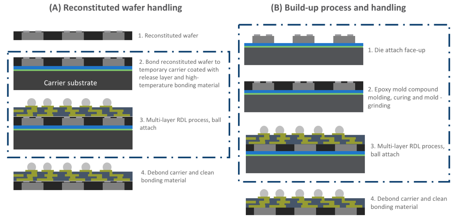
Figure 1. Shows the generic process flow of two predominant approaches for chip-first processes using a carrier-assisted approach. (A) Reconstituted wafer handling and (B) build-up process and handling. The dotted boxed region shows the role of temporary bonding material during the process.
The chip-first process flow has two generic process routes, reconstituted wafer handling and build-up process and handling. Figure 1 shows the general schematic process for both of these process routes. The predominant differences in both of these routes occur during the reconstituted wafer building. In process route A, reconstituted wafer handling, the wafer is built on a separate carrier and then transferred to a 2ndcarrier coated with a high-temperature temporary bonding material and a release layer for subsequent RDL-build up and assembly. In process route B, the chip attach, reconstitution, RDL-build, and assembly processes happen on a single carrier coated with a high-temperature-compatible temporary bonding material and a release layer.
The principal challenges for a temporary bonding material used for chip-first type process include warpage control, die shift, temperature stability, etc., and these were addressed in a previous publication [2]. The chip-first fan-out process is now used in high volume with increasing usage to support mobile electronics applications.
RDL-first/chip-last FOWLP
Figure 2 shows the schematic drawing of a RDL-first FOWLP process. Here, the processes for the RDL layer and the assembly processes for die attach are done on a temporary carrier coated with a sacrificial release layer. Typically, a glass carrier is coated with a release layer and then a series of process steps are completed for creating the RDL layer. These steps are repeated multiple times to create a multi-layer RDL structure. After the RDL process is completed, the wafers go through assembly process steps involving die attach, molding, and mold grinding, followed by carrier release. The preferred method for carrier release on a wafer level, for RDL-first type processes, uses a laser release mechanism. Many foundries and OSATs are developing this process for advanced integration at both wafer level and panel level.
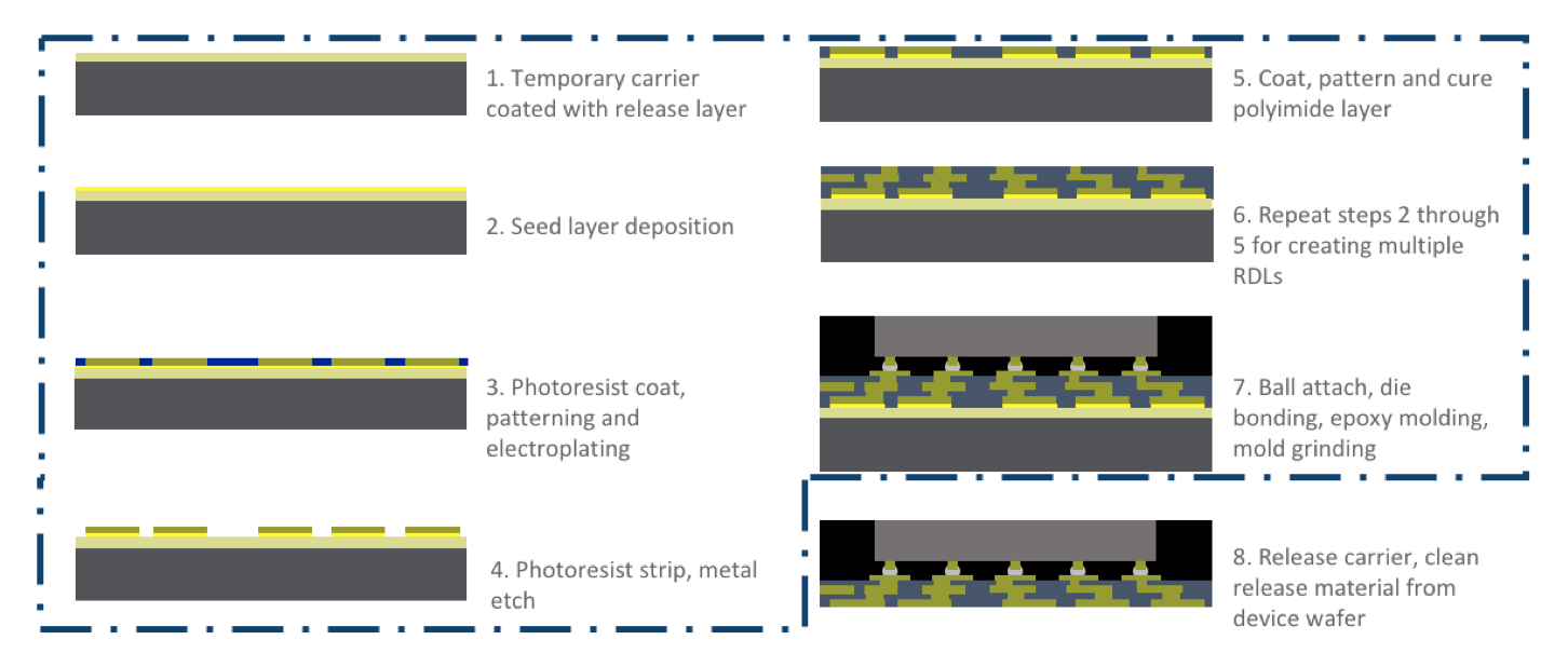
Figure 2. Schematic process flow for an RDL-first/chip-last process. The dotted boxed region shows the role of temporary bonding material during the process.
Critical requirements for sacrificial release material in RDL-first process
The sacrificial laser release layer is coated on a carrier, and it serves as a layer on which the subsequent redistribution layers, chip-attach, assembly, and molding processes take place. This material serves as a foundational material on which all the other layers are built as opposed to serving a singular function of an adhesive layer or a release layer. Compared to the chip-first process, the RDL-first process is harsher on the sacrificial release layers because the full face of the release layer is open to process chemicals during the early steps of RDL formation. The release layer needs to have good adhesion to metal seed layers and/or polymer dielectric layers depending on the specific process flow. The release layer must also have good chemical resistance against photolithography chemicals, metal etch chemistries, and various other solvents in open-face testing. Moreover, the release layers need to withstand high-temperature processing during polyimide curing steps for extended periods and avoid flowing during high-temperature and high-pressure die-attach processes and epoxy molding of the dies. Figure 3 shows the critical requirements of a sacrificial release layer for RDL-first processes. It is important to note that calling this material a sacrificial laser release layer does not capture all the essential functions served by this material.
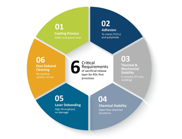
Figure 3. Critical requirements of sacrificial release layer for RDL-first processes
Coating process
The sacrificial laser release layers must be compatible with both wafer-level and panel-level coating techniques. The materials should offer excellent coat quality with uniform TTV across the entire substrate. Some of the risks involved are pinhole defects, dewetting spots, nonuniform thickness, etc. These coating anomalies will have a detrimental effect on the downstream processes.
For example, pinhole defects and dewetting spots would cause the subsequent layers coated on top of the release layer, either a polyimide (PI) layer or a PVD metal, to be in direct contact with the carrier substrate through the pinholes and dewet spots. This will result in poor debonding performance as there will be no release layer in between the carrier and the metal or PI layer to give the release functionality across the defect areas. If the release layer was coated with nonuniform thickness, this will impact release functionality and probably affect the laser absorption capability of the release layer, resulting in transmission of high-energy laser light to to the active device surface during the debonding process, thereby causing potential harm to the devices.
The sacrificial laser release layers developed by Brewer Science are compatible with spin-coating processes for wafer-level application and slot-die coating processes for panel-level application. The materials coat the glass wafers and panels with excellent uniformity without any defects. Figure 4 shows the panel-level uniformity of sacrificial release materials A & B coated using a slot-die coating process.
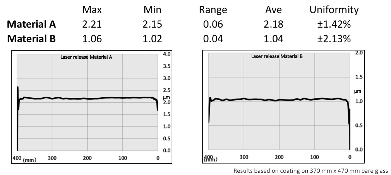
Figure 4. Panel-level coating uniformity of sacrificial release materials A & B coated using a slot-die coating process.
Adhesion
The sacrificial laser-release materials must adhere very strongly to glass, organics like polyimide, and metals like Ti and Cu deposited using a PVD process. Poor adhesion strength will result in delamination of redistribution layers or the built-up device substrate during the assembly process. Apart from the characteristic of the release layer, specific metal deposition processes have also known to have an impact on adhesion strength. Best practices for metal deposition should be followed to improve adhesion to the release layer.
We tested the adhesion of our laser release materials A & B to PVD Cu using a cross-hatch tape test standardized by ASTM-D3359. Figure 5 shows the results of the cross-hatch adhesion tests of Cu on both materials. A poor adhesion would have resulted in the peeling off of the Cu squares created by the cross-hatch pattern, but here the results show excellent adhesion of all Cu squares to the release layers after the tape test.
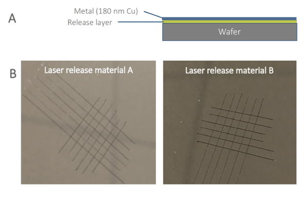
Figure 5. (A) Schematic representation of the test structure for adhesion tests and (B) results of the cross-hatch adhesion tests of Cu on both release materials A & B
Thermal and mechanical stability
Critical requirements for a sacrificial release layer include thermal and mechanical stability through the build-up process. The RDL layers built on top of the release layers require curing temperatures in excess of 250°C for ~1-3 hours per layer. So, a 3-layer RDL structure would expose the release layer to up to 9 hours of high-temperature process cycles. During the thermal cycles, the release layer should not soften or decompose and must remain rigid and stable.
The sacrificial laser release materials A and B are both thermally and mechanically stable materials. Material A is a thermoplastic with high glass transition temperature (Tg) of 320°C and thermal decomposition temperature (Td) of 410°C. Material B is a thermoset with a Tdof 270°C, and does not exhibit a Tgin the temperature range below Td. These characteristics cause the material to not soften or decompose during high temperature processes during PI curing.
Chemical stability
The sacrificial release layers need to withstand harsh chemical conditions, much of it in the open face, as the release layer would come in direct contact with several of the process chemicals including wet etch chemistries during the build-up of RDLs. Typical chemicals would involve solvents, metal etch chemicals, resist strippers, plating chemicals, and other assembly process chemistries. The release layers must not dissolve, lose thickness, or contaminate the chemical baths encountered during the process. Common methods to study chemical resistance are visual inspection, thickness measurement of release layer pre- and post-chemical exposure, and measurement of changes in plating rate or etch rate of process baths before and after immersion of substrates coated with release layers to detect any contamination or leaching of release layers into the baths.
We studied the chemical stability of the release layers by coating the release layer on Si wafers then subsequently immersing the wafer in respective chemicals followed by a visual inspection and/or thickness measurement. For tests involving visual inspection, only one half of the wafer was immersed in the chemical and to observe any detrimental effects on the coating (color change, adhesion loss, thickness loss, etc.) in the immersed area compared to area that was not immersed in the chemical. Figure 6 shows the results from chemical exposure study on laser release materials A & B and Table 1 shows additional chemical resistance studies conducted on material A.
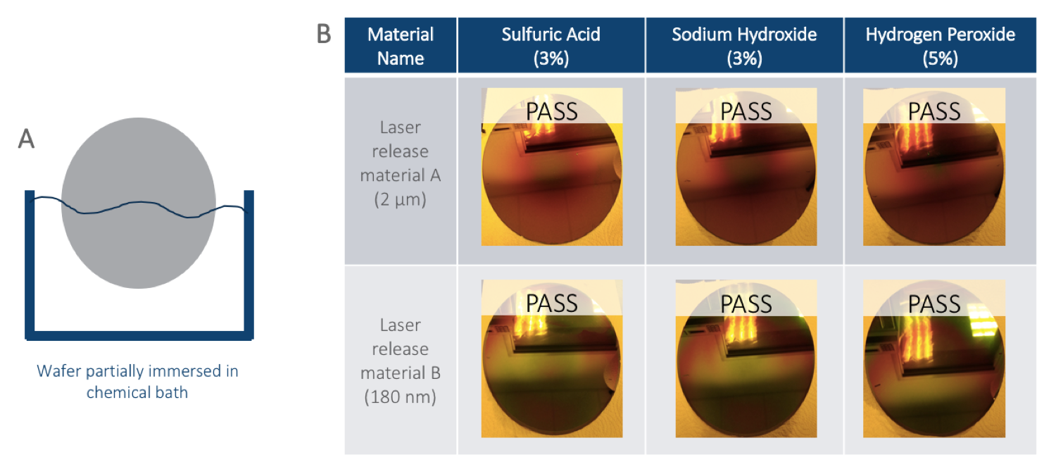
Figure 6. Chemical resistance study (A) schematic representation of a wafer partially immersed in a chemical bath and (B) photographs of wafers coated with laser release material A & B after exposure to chemicals
| Chemicals | Thickness before | Thickness after | Remarks |
| NMP 90 °C 25 min | 2.44±0.19µm | 2.61±0.11µm | pass |
| 2% ammonia 10 min | 2.39±0.03µm | 2.34±0.03µm | pass |
| 2.5% TMAH 10 min | 2.24±0.13µm | 2.24±0.32µm | pass |
| PGMEA 10 min | 2.29±0.33µm | 2.31±0.33µm | pass |
| Buffer HF 3min | 2.27±0.01µm | 2.27±0.02µm | pass |
Table 1. Expanded chemical resistance study using laser release material A
Laser debonding
Laser debonding is the preferred debonding method for RDL-first processes and is a critical process leading to the release of the fully built-up device wafer. Any excursion or defect in this process would result in yield loss of the expensive device wafer. The focus of the laser debonding process is to have no damage to the device wafer and have a high-throughput debonding process with minimal residue. Literature suggests that in UV-laser-based debonding, ablation occurs predominantly due to photochemical breakdown of the organic laser release material as opposed to a photothermal breakdown that occurs in ablation using a longer-wavelength laser source. The sacrificial laser release layers absorb the UV laser light and dissociate chemically to release the carrier from the device wafer. The photochemical ablation process results in less thermal impact on the device wafer and the ablation happens at the interface of the carrier and the laser-release material. The sacrificial laser-release materials developed by Brewer Science are compatible with all the common UV laser debonding tools (308 nm, 343 nm and 355 nm) available in the market for wafer and panel debonding. Figure 7 shows the debonding results of material A and B using the 355-nm laser wavelength.
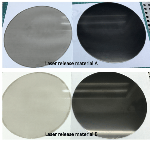
Figure 7. Debonding of laser release material A and B using 355-nm laser source
Post-debond cleaning
After the laser debonding process is completed, it is essential to clean all the release layer residues from the device wafer. Material A is a thermoplastic release layer and it is compatible with both solvent cleaning processes and a plasma cleaning processes. Material B is a thermoset release layer and it is compatible with a plasma cleaning process. The important aspects of the post-debond cleaning process is to completely remove the residues using a cost-effective and short cleaning procedure.
We used a parallel plate plasma etcher to clean the laser debond residues for materials A and B. Table 3 shows the recipe used for plasma cleaning. Both materials are readily cleaned by oxygen plasma. Material A can also be cleaned using a solvent clean using either NMP or dioxolane as solvent in a spin- or a spray-cleaning tool.
| Material | Thickness | Gas (sccm) | Time (seconds) | Power (W) | Pressure (mTorr) | DC-Bias | Results |
| 2 µm | O2-50 | 600 | 150 | 100 | 396 | clean | |
| 180nm | O2-50 | 60 | 150 | 100 | 396 | clean |
Table 2. Recipe for plasma cleaning of laser release material A & B
Summary
From the above list of process requirements for RDL-first fan-out packaging, it can be easily argued that the laser release layer is the one of the critical materials that enable the RDL-first process. The examples in the article showcased the performance of our laser release materials A & B, but we have also developed several other formulations and thickness variations to suit the needs of individual customers and process flows. One such material variation was used to demonstrate a full-flow RDL-first process at our partner site and the results of this full-flow process have also been published recently [3]. The experiment was done on a wafer level using a glass carrier where a multi-layer RDL was built, followed by die attach, molding, debonding, cleaning, and singulation of the dies. The electrical performance of the final device was tested to confirm that no damage occurred to the dies or electrical circuits during the laser debonding process.
As we surpass the age of Moore’s law and enter the era of “more than Moore,” each electronic device is integrated with multiple functionalities for sensing, processing, data transmission, display, etc. Here, heterogeneous integration and system in package (SiP) technologies play an important role in meeting the demands of the end users. Mobile electronics, IoT applications, and other connected services will continue to drive the performance requirements of semiconductor products, and advanced IC packaging processes will increasingly become essential to meet these needs. As an advanced material supplier and an integral part of the semiconductor supply chain, we understand that transformational innovation in materials is key to sustain and support the development of next generation of electronic devices.
References
- Campos et al, “Temporary wafer carrier solutions for thin FOWLP and eWLB-based PoP”, Chip Scale Review, Jan-Feb, 2016.
- Ramachandran K. Trichur et al, “Process Challenges for Temporary Bonding Materials used in Advanced Fan-Out Device Packaging”. Chip Scale Review, Jul-Aug, 2017.
- Wei-Wei Shen et al, "Process Development and Material Characteristics of TSV-Less Interconnection Technology for FOWLP," 67th Electronic Components and Technology Conference; May 30 – June 2, 2017; Florida, USA.
Biographies
Ramachandran K. Trichur received his M.S. in Electrical Engineering from the University of Cincinnati and B.S. in Electrical and Electronics Engineering from Bharathidasan University and is a Director of Business Development at Brewer Science Inc.; email rtrichur@brewerscience.com
Rama Puligadda received her M.S. in Chemical Engineering from the University of Cincinnati and an M.S. in Chemistry as well as a M.Tech. in Polymer Science and Technology from the Indian Institute of Technology and is the Executive Director of Advanced Technologies R&D at Brewer Science, Inc.
Tony D. Flaim received his Ph.D. in Physical Chemistry from the University of Missouri-Rolla and B.A. in Pre-Medicine from University of Missouri-Columbia and is the Chief Technical Officer at Brewer Science, Inc.


Subscribe to Our Blog