
Advanced packaging requires pitches below 10-µm.
Hybrid bonding is the key to paving an innovative future in advanced packaging. Hybrid bonding provides a solution that enables higher bandwidth and increased power and signal integrity. As the industry is looking to enhance the performance of final devices through scaling system-level interconnections, hybrid bonding provides the most promising solution with the ability to integrate several dies with small interconnection pitches below 10 µm. Understanding the basics of hybrid bonding requires asking three fundamental questions: What is hybrid bonding, why use hybrid bonding, and which material is best suited for your application?
You can learn more about Brewer Science’s bonding techniques on our website, or schedule a call with an expert. For a more in-depth understanding of hybrid bonding, please download the white paper, which provides thorough research on the differences between a new polymeric material in comparison to using silicon oxide as the dielectric. The white paper presents material characterization, process optimization, reliability, and preliminary polymer/polymer hybrid bonding results.
What is Hybrid Bonding?
Understanding hybrid bonding requires a brief history of the advanced packaging industry. When the electronics packaging industry evolved to three-dimensional packaging, microbumps provided vertical interconnects between chips by using small copper bumps on dies as one form of wafer-level packaging. Bumps range in size, from 40-µm pitch to eventually being scaled down to 20-µm or 10-µm pitches. However, this is where the issue arises; scaling down past 10µm becomes very challenging and engineers are turning to a new solution to continue to scale size smaller. Hybrid bonding provides a solution for 10 µm pitches and below by completely avoiding the use of bumps, and instead connects dies in packages using small copper-to-copper connections. It provides superior interconnect density, enabling 3D-like packages and advanced memory cubes.
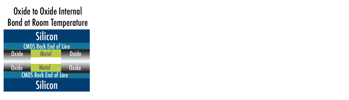
Hybrid bonding is a permanent bond that combines a dielectric bond (SiOx) with embedded metal (Cu) to form interconnections. It’s become known industry-wide as direct bond interconnect (DBI). Hybrid bonding extends fusion bonding with embedded metal pads in the bond interface, which allows face-to-face connection of the wafers.
Why use hybrid bonding?
Hybrid bonding vertically connects die-to-wafer (D2W) or wafer-to-wafer (W2W) via closely spaced copper pads. While W2W hybrid bonding has been in production for several years in image sensing, there is a strong industry push to expedite the development of D2W hybrid bonding. This development will further enable heterogeneous integration, which provides a powerful and flexible means to directly connect die of different functions, sizes, and design rules.
Hybrid bonding offers many advantages over other bonding techniques, including:
- Allows advanced 3D device stacking
- Highest I/O
- Enables sub-10-µm bonding pitch
- Higher memory density
- Expanded bandwidth
- Increased power
- Improved speed efficiency
- Eliminates the need for bumps, improving performance with no power and signal penalties
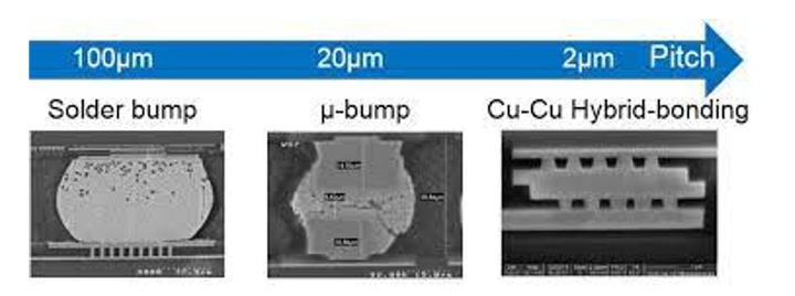
Image Credit: Imed Jani. Test and characterization of 3D high-density interconnects. Micro and Nanotechnolo- gies/Microelectronics. Université Grenoble Alpes, 2019. English. NNT : 2019GREAT094 . tel- 02634259
Inorganic vs polymeric dielectric materials for hybrid bonding
The main differences between SiOx/metal hybrid bonding and polymer/metal hybrid bonding are illustrated in the interactive chart below.
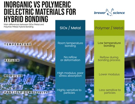
Chemical mechanical polishing (CMP) is one of the key processes in wafer-level packaging. CMP is a process that removes materials by a combination of chemical and mechanical actions to achieve highly smooth and planar material surfaces. Achieving a planar surface through a CMP process is expensive, which is one of the shortcomings of using SiOx as the dielectric material. SiOx requires a planar surface roughness (Ra) of less than 1 nm through CMP. Not achieving a planar surface can be detrimental, as particles or Cu dishing will cause voids in bond lines. Additionally, SiOx has no reflow during bond which can cause air gaps around the metal.
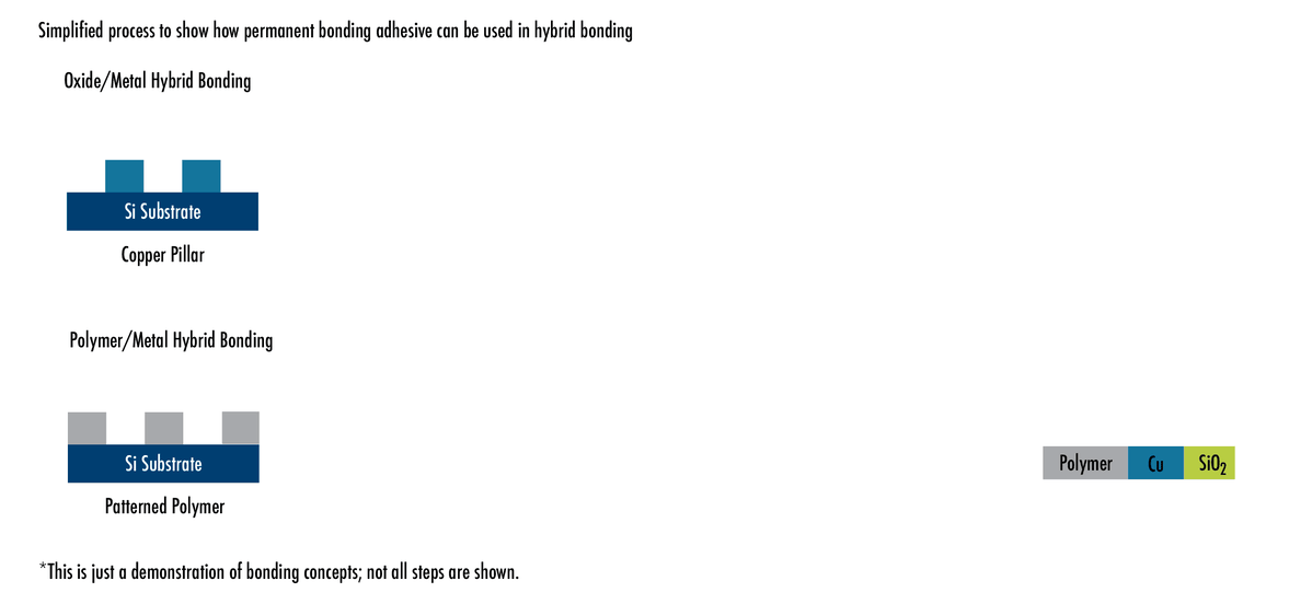
Below is a simplified process to show how a permanent bonding adhesive can be used in hybrid bonding. In case A, a dielectric polymer is applied over Cu pillars and then planarized before bonding. In case B, the polymer is patterned and the Cu pillar is formed via a dual damascene approach before bonding. The functionality of a photopatternable dielectric material makes this flow possible.
Hybrid bonding is an innovative technology being developed for next-generation packaged devices. The latest photosensitive permanent bonding material will be an enabler and complement Brewer Science’s permanent bonding expertise.

Subscribe to Our Blog