
With the explosion in demand for devices that include features in the tens to hundreds of microns, wet-etching is seeing new relevance. Light-emitting diodes (LED), microfluidic devices, ink-jet printer heads, sensors, and many other devices are being mass produced in semiconductor-fab-like environments. However, these feature sizes often do not demand the precision, of plasma etching, nor can they tolerate the cost.
One challenging reality of wet etching is that the entire wafer is exposed to the etchant. To advance the use of such cost-effective batch processing, etch protection schemes must be employed. Brewer Science’s ProTEK® materials are spin-applied polymeric coatings engineered to withstand commonly used etchants, enabling myriad protection strategies.
Blanket Etch Protection
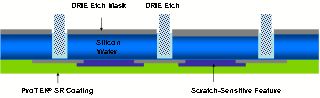
Blanket protection refers to coverage of an entire wafer surface and can even include wafer edge protection. Blanket protection is also discussed in a previous blog article describing its use in deep reactive ion etching (DRIE).
Patterned Etch Protection
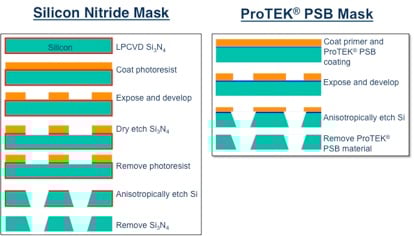
Sometimes blanket protection is not needed. It is often desirable to etch specific areas on a wafer surface while protecting others. Photosensitive protective materials, such as ProTEK® PSB coating, address this need. An increasingly common example occurs in the manufacture of high-brightness LEDs (HB LEDs). To improve light extraction, the surface of the light-emitting material is roughened using a harsh wet-etching process. However, other elements of the device (e.g., metal pads) would be damaged during the etch.
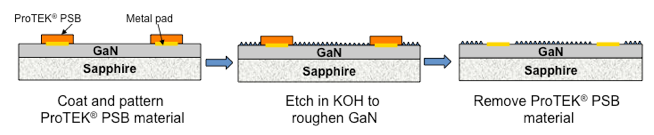
ProTEK® PSB coating can be pattern-exposed and developed to cover only these sensitive elements, and can be subsequently removed without damaging the device.
Conclusion
Processes utilizing the ProTEK® family of materials and processes enable surface etch protection, patterned etch protection, and edge protection. These materials can be used in combination to address a wide range of processing needs, providing lower-cost options to device manufacturers.

Subscribe to Our Blog