Limitations of Moore's Law
Ultimately, performance of computers and other electronic products will be limited by transistor size and density. Because the semiconductor industry has pushed to create ever-smaller features with photolithography, engineers have been able to shrink transistors far beyond original expectations to dramatically increase the density of transistors on a chip, thereby enabling the phenomenal leaps we have seen in the functionality and speed of electronics. However, the rate of performance improvements has become slower than originally predicted by Moore’s law because of the length of the connections between transistors and between individual semiconductor devices in components.
Increasing computing speed with through-silicon vias (TSVs)
Using through-silicon vias (TSVs) to directly interconnect semiconductor chips offers the promise of even greater functionality and faster computing speeds. Recent studies have indicated that computing speed may be increased by more than 10 times by using TSVs, and the associated decrease in inductive losses will reduce power consumption by more than 70%.
Implementation of TSV production requires the ability to handle and process ultrathin wafers as if they were at their full thickness. Most frequently, the full-thickness wafer is mounted on a rigid carrier using an adhesive that at later stages allows separation of the thin device wafer, which contains TSVs, from the carrier and removal of the adhesive. Although wafer-to-wafer bonding has been in use for some time for permanent bonding applications, and waxes have been used to bond wafers to carriers for thinning and subsequent removal, these processes have not been developed and optimized to allow further processing on the thinned wafer back side and permit separation from the carrier.
Supply chain options for 3D device packaging
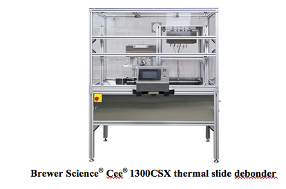
Flexible options for temporary wafer bonding processes, with a variety of investment options, are available for 3DP applications. Device wafers can be mounted, demounted, and cleaned utilizing cost-effective equipment solutions. While mounted to carriers, device wafers may be thinned and may undergo backside processing as needed to create TSVs. Track-quality equipment performance enables scale testing of bonding, debonding, and cleaning processes. This flexibility, and the choice to select from a variety of options, creates a confidential pathway for completing thinned wafer processing feasibility work. Development time is reduced and the introduction of new 3DP applications to the market is accelerated.
For high-volume manufacturing (HVM) environments, Brewer Science has partnered with HVM equipment suppliers to qualify materials and processes for thin wafer handling needs. Customers can select an equipment supplier of their choice, one that can best meet their needs and provide the needed throughput and compatibility with their existing production environments. These suppliers offer equipment for mounting device wafers to carriers and then separating and cleaning the thinned wafers for final packaging.
Brewer Science technology provides customers flexibility for device development, process confirmation, and eventual scale to production.


Subscribe to Our Blog