
Thin-wafer processing trends
Several spin-coating process applications require the ability to uniformly coat, develop, and/or rinse (clean) thinned and fragile substrates. Safely handling these fragile materials is paramount and requires specially designed spin chucks and thin-wafer handling techniques. The substrates are made of a wide array of materials, and some of the more popular ones include flexible polymer films (for example, fluorinated ethylene propylene [FEP] and polyester [PET]) and metal foils (titanium, aluminum, and steel). These materials are common for markets within the optics, thin-film transistor (TFT) display, and photovoltaic (PV) industries. Thicknesses of the substrates often range from 50 to 100 µm (0.001 to 0.004 inch) and are cut into various shapes (round, square, and rectangular).
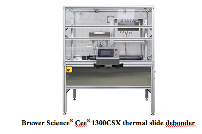
Moreover, we are seeing a growing migration in the microelectronics industry toward through-silicon via (TSV) technology for 3-D wafer stacking. This technology requires significant reduction in substrate thickness and exponentially increases the complexity of handling for every subsequent processing step. The thinned substrate materials include silicon for advanced packaging as well as compound semiconductor (CS) materials including gallium arsenide (GaAs), gallium nitride (GaN), indium phosphide (InP), and silicon carbide (SiC) for high-power radio-frequency (RF) devices and light-emitting diodes (LEDs). The CS and III-V materials are extremely brittle and far more sensitive to both mechanical and thermal shock. Film frames are commonly used to support silicon (Si) and CS materials. A device wafer can be mounted onto a film frame after backside processing but while it is still supported by its carrier, as in the Brewer Science® ZoneBOND™ process, or following separation (debonding) from the carrier, as in the thermal slide debonding process, for subsequent transport, cleaning, and packaging.
Issues with standard vacuum spin chucks
Process engineers often encounter a major hurdle with standard vacuum chucks that use a series of concentric circles and/or small-diameter perforated holes to supply vacuum through the spin chuck surface. These designs distribute the vacuum unevenly across the surface and cause dimples, deflection, and/or, in worst-case scenarios, cracking. Furthermore, all of these detrimental anomalies will lead to less-than-optimal film characteristics across the substrate. A film frame support structure will assist in handling these delicate films; however, any irregular chuck topography will detrimentally affect total thickness variation (TTV). Therefore, specialized spin chucks are recommended to safely contact thinned substrates without risk to delicate structures and subsequent film uniformity.
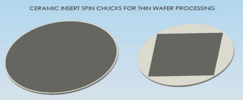
Alternative spin chuck designs
For thinned substrates (< 250 µm thick), we have developed a porous ceramic insert design that has a distinct advantage of completely supporting the backside of any given substrate dimension. The chuck distributes the vacuum equally through a porous surface and mitigates any potential deflection, eliminating detrimental effects to your substrate or coat quality. These chucks are design specific and available for a wide array of shapes and sizes.
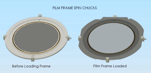
The porous ceramic design can also be adapted for thinned substrates mounted to film frames. Mechanical clamps and a porous ceramic insert combine for spin processing thinned substrates (< 250 µm thick) that have been taped to frames. The ceramic insert ensures complete and uniform backside support, while it distributes the vacuum source across the taped surface. This design also utilizes vacuum O-rings and mechanical clamps for securing the outer film frame to the chuck assembly and maintaining positive lock.
Although these chucks enable safe handling of ultrathinned substrates, they are exponentially heavier and create significantly more inertia than standard round vacuum chucks. To achieve adequate acceleration rates, these chucks can only be used on spin coaters with high-horsepower drive systems. All Brewer Science® Cee® spin coaters feature the industry’s highest-horsepower servo-motor indirect drive system and will allow the direct transfer of standard spin processing conditions. This system delivers the unique capability of combining porous ceramic chuck technology, existing high acceleration rates, and multiple spin-speed steps to fully optimize your thin-wafer processing application.

Subscribe to Our Blog