
Through-silicon vias (TSVs) are becoming increasingly common for high-speed and high-bandwidth connections on a chip. TSVs are especially important in 3D packaging schemes and are also used in many sensor, MEMS, and LED devices.
While it is common to use deep reactive ion etching (DRIE) for creating the TSVs, wet etching of the silicon to create vias is a cost-effective process. In contrast to DRIE’s single-wafer processing that uses more expensive plasma etching equipment, wet-etch TSV formation allows batch processing using relatively inexpensive equipment (wet processing baths).
Etch mask challenges
One of the main challenges in wet etching of silicon is availability of a cost-effective etch mask scheme for protection during etching.
Conventional schemes for etch masks include chemical-vapor-deposited (CVD) silicon nitride (SiN) or silicon dioxide–based etch masks. The mask process involves several steps including specialized tools for high temperature CVD processing and dry-etch processing apart from the use of standard photolithography tools. The masking process and required toolset effectively raise the cost of ownership (CoO) of a wet-etch process, which would otherwise be a cost-effective option for users.
Brewer Science presents an elegant spin-on etch mask solution that minimizes the number of steps used for creating an etch mask and avoids the use of CVD-based tools for etch mask creation. The etch mask offers complete protection without pin-holes or delamination during silicon etching using alkaline etch baths (potassium hydroxide [KOH] or tetramethyl ammonium hydroxide [TMAH]).

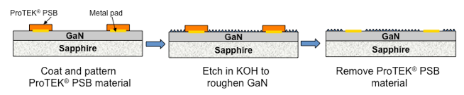
Figure 1. Comparison of etch mask process scheme for wet-etch protection using (a) silicon nitride mask and (b) ProTEK® PSB spin-coatable etch mask
Cost-effective TSV creation
We have created TSVs using ProTEK® PSB photosensitive material for etch protection. The process provides good control and etch pattern integrity that is suitable for commercial production of TSV wafers for advanced interconnect structures.
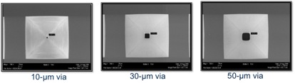
Figure 2. SEM images showing TSVs of various dimensions created using ProTEK® PSB coating as an etch mask
Brewer Science® ProTEK® materials can protect entire surfaces and serve as effective etch masks for creating TSVs and other microstructures on silicon using wet etching. ProTEK® products provide a low-CoO option compared to conventional CVD-based etch mask techniques. As wafers become thinner, wet-etch TSV formation becomes more viable, providing a low-cost option to device manufacturers.

Subscribe to Our Blog