
As semiconductor devices evolve, smaller and smaller feature sizes are required to achieve the performance desired by the consumer. Smaller features give rise to lower power consumption for mobile devices, less expensive devices due to the ability to manufacture more chips per wafer, and faster overall speed.
Why multilayer?
Smaller feature sizes also lead to higher aspect ratios in the photoresist, which cause pattern collapse and result in smaller processing windows. Therefore, photoresists have become thinner to offer higher resolution and to overcome pattern collapse. Typical photoresist thicknesses for today’s cutting-edge immersion processing are in the range of 60 nm to 100 nm, whereas typical photoresist thicknesses just a few years ago were about 150 nm. The trade-off for using thinner photoresists is a smaller etch budget for pattern transfer into the substrate. For this reason, multilayer patterning is needed.
How multilayer patterning works
Current multilayer patterning uses a thin photoresist with a thin inorganic or organometallic etch barrier layer (a hardmask, HM) that is deposited by either chemical vapor deposition (CVD) or spin-coating processes over the top of a thicker layer that is high in carbon content (a carbon hardmask, CHM). Some examples of CVD hardmask layers include SiON, SiN, and TiN. Organosilicates are one example of a spin-on hardmask. An example of a carbon hardmask applied by CVD is alpha-carbon. Spin-on carbon (SOC) hardmask layers consist of organic polymer solutions that are high in carbon content by design.
High inorganic content in the hardmask layer is important for transferring the photoresist image through the multilayer stack. High inorganic content allows for faster plasma etching in a fluorinated etch gas, thus reducing the photoresist thickness required to pattern the hardmask. High inorganic content also slows the hardmask etch rate in oxygen plasma so that the hard mask maintains its integrity while transferring the photoresist pattern into the carbon hardmask layer.
High carbon content in the carbon hardmask layer is important because carbon etches slowly in the plasma gases typically used to etch into inorganic substrates such as silicon, polysilicon, SiO2, and low-k dielectrics.
Multilayer processing with spin-on coatings is a simpler process than CVD multilayer processing. The entire multilayer stack is applied in the coating module of a track, which eliminates the need to transfer wafers to another module for deposition.
OptiStack® multilayer systems
Brewer Science® OptiStack® systems simplify the overall lithography process by offering a universal lithography platform that eliminates topography dispersion and maintains optimal optical interfaces in the same focal plane, regardless of the substrate optical properties.
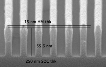
OptiStack® HM710 material on OptiStack® SOC110D material. High etch selectivity permits very thin hard mask and straight profiles.


Subscribe to Our Blog