
 Richard Feynman, who won the Nobel Prize in Physics in 1965, gave a famous lecture titled “There's Plenty of Room at the Bottom.” Today’s microelectronics process engineer, in the context of conventional top down lithography, would find it difficult to accept this statement without a long list of caveats. Aggressive scaling demands for newer generations of microprocessors have led to extremely tight budgets for tolerances on device dimensions and device placement on a chip, among other challenges. One may argue that there is very “little room at the bottom” for error.
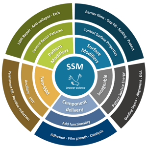
The industry has come up with many creative and innovative ways to address these scaling challenges. One of these being bottom up approaches, as in, building device relevant features from the bottom up. These include directed self-assembly (DSA), other self-aligned methods, and more recently area-selective deposition (ASD). These fabrication tools allow us to innovate outside of the scope of conventional lithography and use unconventional methods to circumvent the challenges that plague older technologies.
The Selective Surface Modification (SSM) group at Brewer Science, along with its partners at imec and other industry leaders, develops materials and processes that enable these bottom-up approaches for industrial scaling. We have recently developed novel materials and processes for surface selective etch modification. These materials, along with the processes, can differentiate between various surfaces and selectively impart desirable etch properties to the surface beneath. We have demonstrated that this concept can be applied to block copolymers, such that one of the blocks of perpendicularly oriented lamella structures can be selectively given slower etch properties. This selective etch property modification enables easier etch transfer into substrates for device manufacture.
Brewer Science continues to innovate at the frontier of semiconductor manufacturing from our multilayer technologies such as OptiStack® materials to DSA and selective surface modification for bottom-up approaches. For more information about this work contact us at info@brewerscience.com or visit https://www.pathlms.com/avstechnicallibrary/events/988/slide_presentations/97630.


Subscribe to Our Blog