
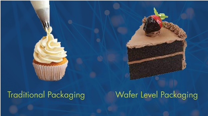
“Just the tip of the iceberg.”
What a great saying. It means what we can see pales in comparison to what we can’t.
In the world of technology, people often marvel at the end product but rarely consider the extremely important advances and transitional processes that make it all possible. As smaller chip sizes and higher efficiency at lower costs drive these advances, it’s important to recognize how we got here before we try to take on the future.
The industry is currently in transition when it comes to integrated circuits so we’re going to take a look at 2.5D integration’s role right now and how 3D integration will affect the future.
The importance of 2.5D
In 2008, Christopher Nolan released “The Dark Knight,” the highly anticipated follow-up to the first installment of his Batman reboot, “Batman Begins.” After dark twists and menacing turns, the movie shows Batman becoming the anti-hero, famously expressed as “…not the hero Gotham deserves, but the one it needs right now.”
As the push for 3D integration across the board is at the forefront of our minds, it’s important to recognize 2.5D’s role as not necessarily the hero the semiconductor industry deserves, but the one it needs.
2.5D integration has played a crucial role in transitioning from 2D (think mid-90s cellphones) to the future by allowing ICs to sit closer together and share interconnect space along the same plane. This made a couple of significant things possible:
- Chips took up less space on the board, allowing for more performance-enhancing chips to be placed.
- Signals powering the chip functions had a shorter distance to travel, making the set of chips much more efficient.
2.5D was a huge step in the right direction. But the need for lower cost, higher performance, and longer battery life continue to relentlessly drive demand — and 2.5D is beginning to reach its limitations.
That’s where 3D comes in.
The promise of 3D
Full 3D integration refers to a set of two or more integrated circuits stacked on top of each other with the interconnects embedded within the actual chips by way of through-silicon via (TSV). This kind of integration can significantly free up device real estate and allow for more chips. And since signals don’t need to travel anywhere to reach all the chips, efficiency and performance go through the roof.
The best part? It’s already here.
3D integration first made a splash back in 2011 when Micron came out with a high-capacity “memory cube” constructed of multiple integrated circuits, so it’s not necessarily a new process. However, it poses significant costs that we’re trying to cope with. Construction of the TSV is complex and devices need to be thinned even more to ensure the stacks don’t get too tall. It is a very exciting time in nanotech. Things are moving quickly and we’ve got a front-row seat. We’re working every day to develop new processes and equipment to help the industry transition into the future.

Subscribe to Our Blog