
Developing photosensitive film layers to produce features of targeted sizes is a critical process step within any photolithography application. Application engineers have created several processes for performing this step with tank immersion (that is, a bath) and/or several adaptations of spin developing a single wafer to make patterns of features based on film areas of differing solubility. The use of immersion tank processes has steadily declined in MEMS fabrication and advanced lithography over the past decade due to excessive material consumption, non-uniform resolution, and poor clearing from high-aspect-ratio features due to insufficient agitation. Additionally, increased throughput requirements and smaller critical dimensions (CDs) have further shifted mainstream applications to single-wafer (track) spray/puddle process flows.
The standard developer materials consist of low-concentration (< 3%) bases and acids (TMAH, KOH, lactic acid in aqueous solutions). Other popular solvent-based photoresists, dry films, and polyamides are typically resolved and rinsed with polar solvents including propylene glycol monomethyl ether acetate (PGMEA), propylene glycol monomethyl ether (PGME), acetone, and isopropanol (IPA).


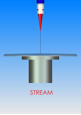
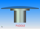
The most common single-wafer process is designed to deposit the developer solution onto the center of the wafer surface through a stream puddle technique. The wafer is then spun at low speed (0-50 rpm). The rotation is then stopped and held at 0 rpm to enable the material to “puddle” and allow the chemical reaction to actively dissolve the soluble areas of the patterned film. This process is very popular for thin films ≤ 1 μm thick and/or for small wafer applications. For thick films and/or high-aspect-ratio features, the stream puddle step may be repeated over several iterations to reapply fresh developer. However, because this method of development is inherently non-uniform, it can be problematic for many thick-film and large-surface-area processes. Often features along the wafer perimeter are underdeveloped, and center features are often over-exposed.
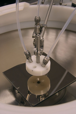
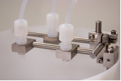
The use of side-angle spray nozzles significantly enhances fluid deposition uniformity. The standard configuration utilizes two side-spray, V-line spray nozzles to evenly apply developer solution and deionized (DI) water across the substrate simultaneously. Some configurations use an open UHMW polyethylene lid with spray nozzles mounted either outside the wafer plane, spraying inward from the center of the wafer out (puddle spray), or directly over the substrate for continuous (direct) spray applications. The side spray nozzles are factory positioned outside the wafer plane (side orientation) and ensure uniform deposition for all substrate sizes (2-8 inches). The spray nozzles can also be used in a puddle developer application by quickly applying material to the substrate at a slow speed and then reducing the substrate speed to 0 rpm. Programming and setup options will also enable continuous-spray applications with the omission of all static (0 rpm) steps during the recipe and spray continuously throughout processing steps.

Many of the latest specialized lift-off resists and dry films (MicroChem LOR and SU-8 resists and Shipley BPR™-100 resist) are not compatible with spray/stream puddle development and require immersion, continuous direct-angle spray, and/or megasonic-assisted processes. Immersion methods are less than ideal and are not preferable for the reasons mentioned above. Direct-angle nozzles are often used for continuous-spray applications and allow accelerated development of thick films (5-100 μm) with features having high aspect ratios. The direct angle provides sufficient agitation to penetrate the film and remove soluble material. Another distinct advantage of this method is the continuous replenishment of fresh solution to accelerate development.
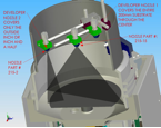
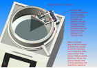
Introduction of megasonic development was a dramatic technology leap in this area. This development/cleaning technology combines a ProSys MegPie megasonic transducer with spray/stream developer systems. The radial megasonic array is specifically designed to apply uniform acoustic energy across the entire surface of the spinning substrate and gently lift away soluble materials without damaging fragile structures. This technology is uniquely suited to resolve extremely small CDs with high-aspect-ratio (> 5:1) structures for MEMS fabrication and advanced lithography (193- and 248-nm).
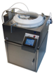
The Brewer Science® Cee® equipment line has been specifically engineered to accommodate all spin-developer process techniques including stream, spray, direct-angle, and megasonic-enhanced. As the predominant lab-scale equipment supplier for advanced R&D and prototyping, the Brewer Science® Cee® product team is eager to meet your specific application needs.


Subscribe to Our Blog