
In recognition of its progress with temporary bonding and thin wafer handling, Brewer Science was featured in the November/December issue of Chip Scale Review.
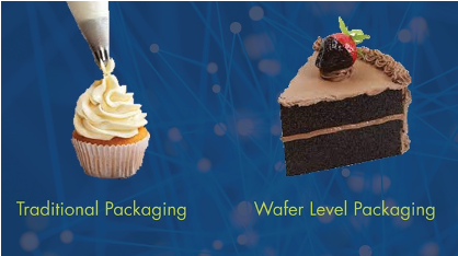
The feature discusses the company’s use of wafer-level packaging (WLP) technologies in semiconductor segments, including fan-out WLP (FOWLP); fan-in wafer-level chip-scale package (FI-WLCSP); 3-D FOWLP; 2.5-D integration with interposer technology; and true 3-D IC integration using through-silicon via (TSV) interconnects. The authors are Ramachandran K. Trichur, Business Development Manager for Temporary Bonding, and Dr. Tony D. Flaim, Chief Technical Officer.
Brewer Science offers bonding and debonding materials, as well as wafer-handling expertise and on-site equipment setup and training. Its goal? Helping device makers and advanced packaging manufacturers take advantage of cost-efficient and reliable thin-substrate handling technologies to make smaller, faster, more highly integrated devices.
Other points covered by the authors include:
- Depending on market segment, key challenges in temporary bonding include high-stress substrates, the need for wafer support systems during bonding, and the necessity of different bonding temperatures.
- The market for FOWLP reached $200 million in 2014 and is expected to grow at an annual rate of 30 percent. FOWLP packages are expected to become thinner to meet market needs.
- In general, the industry is moving toward higher-temperature processing of thinner, more highly stressed, larger-area substrates and panels.
- Expectations for temporary bonding materials are moving toward more streamlined bonding and debonding processes at lower temperatures and with less force to improve yield and throughput and reduce cost of ownership.
To read more about Brewer Science’s temporary bonding and thin wafer handling strategies, view the article “Temporary bonding and thin wafer handling strategies for semiconductor device processing” at http://fbs.advantageinc.com/chipscale/nov-dec_2015/#40.
Subscribe to Our Blog