
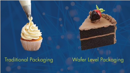
The terms "quantity" and "quality" are often discussed in "either/or" scenarios. On one side, you get a lot of something. On the other side, you get the best of something else. In these scenarios, you can't have both, at least not at the same time. In the semiconductor industry, there is constant innovation and limit testing around these concepts. However, when "quantity" starts inching ahead of "quality," we run into some issues.
As demand increases for smaller chip size, the challenge lies not in how to deliver a smaller chip but how to ensure that quality and performance keep up. One of the biggest issues in quality seems to be interconnect space. Chips are getting smaller, yes, but how can we ensure there's enough room to efficiently and effectively connect them? Embedded wafer-level ball grid array (eWLB) is the semiconductor industry’s most exciting solution. eWLB involves taking a standard chip-laden silicon wafer and dicing and testing the chips, as you normally would. However, after you've found your known good die (KGD), you arrange them in a grid with spaces in between and fill in the spaces between with a specialized epoxy. The resulting structure, in turn, becomes like its own new wafer. This means you're processing a brand new wafer of chips that you know are good, saving you the time, frustration, and significant cost of performing your back-end steps on bad chips. As an added bonus, the epoxy-filled space around the chips allows interconnects to be "fanned-out" on the bottom of the chip, allowing many more interconnects to be added.
Here's a standard wafer-level ball (WLB) grid array we've used without the epoxy:

Now here's what it looks like with the epoxy surrounding the chip and the “fanned-out” interconnects added:

But what are the benefits? According to Juni Myers, Brewer Science's Applications Engineer, these are just the tip of the iceberg:
- More space for interconnects—ensure the quality of the chips you produce handily keeps pace with the rapid decrease in size.
- Concurrent processing on existing equipment—your current process and equipment need not change to incorporate this concept.
- High yields—high efficiency means less waste, high throughput, and big cost savings.
Every new process, of course, comes with its own challenges, which is where we're focusing much of our time and resources right now. Things such as undesirable wafer warpage, the need for materials with thermal stability, and the challenges of debonding present unique obstacles to making this a foolproof process. Brewer Science is working closely with companies to vigorously test the boundaries and limitations of the process and define rigid standards to make implementation seamless in any setting.
But just think of the possibilities: exponentially more responsive sensors, longer battery life, and better chip efficiency, all while minimizing extra costs, waste, and steps. As chips continue to shrink in size in the future, chances are eWLB will play an enormous role in keeping them highly functional and incredibly valuable.
Check out our blog on 3-D stacking and the future of integrated circuits to learn more about the opportunities that keep Brewer Science pushing the semiconductor industry forward.

Subscribe to Our Blog