
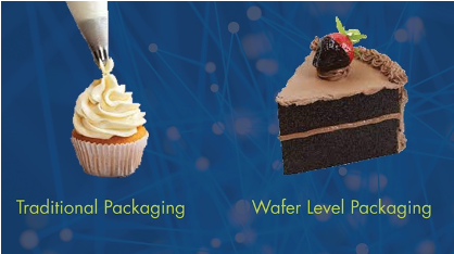
What makes it possible for our smartphones, tablets, gaming systems, networking devices, and everyday electronics to operate at faster speeds, process more information, and continue to shrink in size? Until now, the answer has included a number of advanced technologies and processes that have allowed the microelectronics industry to double the number of circuits in the same two-dimensional space, but the future relies on the emerging innovation of stacked memory and three-dimensional integrated circuits.
To create these new, stacked designs, manufacturers must find ways to thin their device wafers before performing complex back-end processes. The objective is to not damage these very thin and valuable substrates that could potentially comprise tens of thousands of devices on each wafer.
How does temporary bonding work?
Silicon wafers from 2” to 12” in diameter are commonly used throughout the microelectronics industry to construct circuits and memory devices. As the wafers are thinned or exposed to heat, they need to be protected and supported to avoid damage. Using temporary bonding techniques in which the wafer is attached to a stable carrier without disrupting back-end processes can overcome this problem.
These back-end processes could include:
- Mechanical stress
- Grinding
- Polishing
- Stress relief
- Coating and deposition
- Lithography
- Anodic bonding
- Exposure to various chemistries (acids, solvents, etc.)
- Plasma etch and deposition
- Dielectric deposition
- Exposure to ambient gas
- Vacuum
Some processes are more rigorous than others, often requiring the thin wafers to endure extreme heat exposure and mechanical force. Without temporary bonding solutions, the thin wafers would crack under the pressure.
Thin wafer handling process
- Wafers are attached to the "carrier," which can be glass, silicon, sapphire, or other materials.
- The wafer and carrier are bonded using a specific temporary bonding material. The type of carrier and the bonding material used depend on the debonding method.
- Back-end processes are performed.
- Debonding is performed using one of many methods, including chemical release, thermal slide release, mechanical release, and laser release. The release method is chosen based on a number of principles relating to back-end processes and desired maximum throughput.
 Chemical Release |
 Laser Release |
 Mechanical Release |
 Thermal Slide Release |
Brewer Science has not only developed the materials and equipment to bond and debond, but we also provide thin wafer handling expertise with on-site equipment setup and training. Our products and services help all types of electronics perform more quickly and efficiently, providing a unique benefit for all consumers.

Subscribe to Our Blog